
 SkillClick
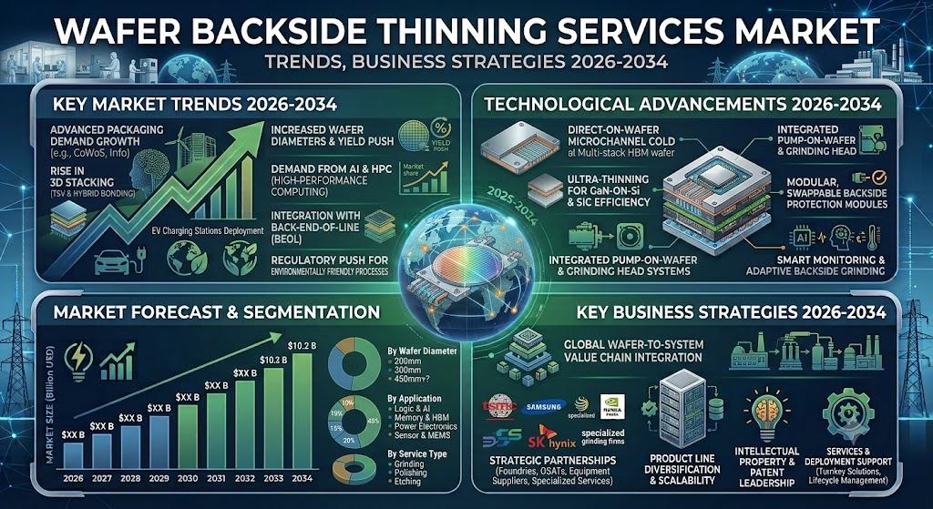
Wafer Backside Thinning Services Market, Trends, Business Strategies 2026-2034
The global Wafer Backside Thinning Services Market is witnessing a pronounced up‑trend as semiconductor manufacturers accelerate the shift toward advanced packaging, 3D‑IC integration, and heterogeneous integration. Growing requirements for ultra‑thin, high‑precision wafers are reshaping the service landscape, prompting both legacy players and emerging specialists to expand capabilities, invest in proprietary equipment, and pursue strategic alliances with leading fabs.
Wafer backside thinning services-encompassing precision grinding, selective etching, and surface conditioning-play a pivotal role in enabling sub‑50 µm wafer thicknesses required for next‑generation logic, memory, and power devices. By reducing wafer thickness, manufacturers achieve higher device density, lower package profiles, and improved thermal performance, all of which are critical for modern consumer electronics, automotive systems, and data‑center processors.
Download FREE Sample Report:
Wafer Backside Thinning Services Market - View in Detailed Research Report
Semiconductor Industry Expansion: The Primary Growth Engine
The report identifies the explosive growth of the global semiconductor industry as the paramount driver for wafer backside thinning demand. With semiconductor fab capacity expanding at a compound annual growth rate (CAGR) exceeding 7 % through 2034, the need for precision thinning services has become a core enabler for high‑volume manufacturing of AI/ML processors, 5G radios, and automotive power modules. The semiconductor equipment market itself is projected to surpass US$ 120 billion annually, creating a sustained pipeline of investment in downstream services.
“The concentration of leading foundries and OSATs in the Asia‑Pacific region, which accounts for roughly 78 % of global wafer processing volume, fuels the most intense demand for backside thinning services,” the study notes. Global capital expenditures on new wafer fabs are expected to exceed US$ 500 billion by 2030, with a substantial portion earmarked for advanced packaging infrastructure that relies on ultra‑thin wafer handling.
Read Full Report: https://semiconductorinsight.com/report/wafer-backside-thinning-services-market/
Market Segmentation: Grinding Dominates, Consumer Electronics Leads Applications
The report provides a detailed segmentation analysis, offering a clear view of the market structure and key growth segments:
Segment Analysis:
By Type
- Grinding
- Etching
- Others
By Application
- Consumer Electronics
- Automotive Electronics
- Computer and Data Center
- Others
By End User
- IDMs (Integrated Device Manufacturers)
- Foundries
- OSATs (Outsourced Semiconductor Assembly and Test)
By Wafer Size
- 200 mm
- 300 mm
- Larger than 300 mm
By Service Provider
- Pure‑play Thinning Specialists
- Integrated Semiconductor Services
- Captive Provider Services
Segment Analysis Table:
| Segment Category | Sub‑Segments | Key Insights |
| By Type |
|
Grinding dominates the market as the preferred wafer thinning technique because:
|
| By Application |
|
Consumer Electronics remains the largest application segment because:
|
| By End User |
|
Foundries are primary users of wafer thinning services due to:
|
| By Wafer Size |
|
300 mm wafers exhibit the strongest demand for backside thinning because:
|
| By Service Provider |
|
Pure‑play Thinning Specialists maintain leadership through:
|
COMPETITIVE LANDSCAPE
Key Industry Players
Global Market Dominated by Specialized Semiconductor Service Providers
The wafer backside thinning services market is characterized by a concentrated competitive landscape, with leading players like DISCO Corporation and Syagrus Systems controlling significant market share through advanced grinding and etching technologies. These established providers maintain dominance through proprietary equipment, precision engineering capabilities, and strategic partnerships with major semiconductor fabs. The top five companies collectively accounted for approximately XX% of global revenue in 2025, with technological differentiation in ultra‑thin wafer processing (sub‑50 µm) serving as a key competitive battleground.
Several specialized manufacturers have carved out strong positions in niche segments, including Silicon Valley Microelectronics for MEMS applications and NICHIWA KOGYO for compound semiconductor substrates. Emerging players such as Huahong Group and Winstek are gaining traction in Asian markets through cost‑competitive service models, while technology‑focused firms like Helia Photonics compete through innovative thinning solutions for photonic applications. Regional specialists like Phoenix Silicon International have strengthened their positions through localized service networks and quick turnaround capabilities.
Regional Analysis: Wafer Backside Thinning Services Market
Asia‑Pacific leads in adopting advanced wafer backside thinning techniques like temporary bonding/debonding and ultra‑thin wafer handling, with Taiwanese firms pioneering sub‑50 µm thinning capabilities for 3D IC applications.
The region boasts the world's highest concentration of 300 mm wafer fabs, creating concentrated demand for high‑volume backside thinning services near major semiconductor clusters in Hsinchu, Shanghai and Pyeongtaek.
Close collaboration between thinning service providers, equipment manufacturers and OSAT companies enables seamless integration from wafer fabrication to packaging, reducing logistics costs and cycle times.
Growing demand for wafer thinning services comes from advanced packaging applications including CIS, MEMS sensors and power devices, with Chinese manufacturers rapidly expanding capabilities for automotive and IoT chips.
North America
North America maintains leadership in specialized wafer backside thinning services for high‑performance computing and aerospace applications. The region benefits from strong R&D capabilities and demand from fabless semiconductor companies that outsource advanced packaging needs. Major IDMs in the United States are investing in wafer‑level packaging solutions to support AI/ML processors requiring ultra‑thin wafers. The presence of leading equipment manufacturers enables access to cutting‑edge thinning technologies, though local thinning service capacity remains limited compared to Asia, leading to partnerships with overseas providers.
Europe
Europe's wafer backside thinning market is characterized by specialized applications in automotive and industrial sectors, with Germany and France leading in MEMS and power device production. The region has developed niche expertise in handling compound semiconductor wafers for RF applications. While lacking Asia's volume capacity, European service providers focus on high‑mix, low‑volume production with stringent quality requirements. Collaborative R&D projects under EU semiconductor initiatives are driving development of advanced thinning techniques for next‑generation power electronics.
Middle East & Africa
The MEA region is emerging as a potential market for wafer backside thinning services, with growing semiconductor packaging activity in Israel and limited foundry operations in the United Arab Emirates. Most regional demand is met through partnerships with global service providers, though local capabilities remain limited. The region shows potential for specialized applications in aerospace and defense sectors, with investments in compound semiconductor manufacturing creating future opportunities for localized thinning services.
South America
South America remains a minor player in wafer backside thinning services, with limited semiconductor manufacturing infrastructure. Brazil hosts modest packaging and test operations that utilize basic thinning services, primarily sourced from international providers. The region's market potential is constrained by limited local semiconductor production, though growing electronics manufacturing could drive future demand for basic backside thinning solutions.
Emerging Opportunities in AI, EV, and 5G
Beyond traditional semiconductor drivers, the report highlights significant emerging opportunities. The rapid growth of AI‑accelerator chips, electric‑vehicle power electronics, and 5G radio‑frequency modules demands ever‑thinner wafer substrates to meet aggressive form‑factor and performance targets. Additionally, Industry 4.0 adoption is fostering smart thinning services equipped with real‑time thickness monitoring, predictive maintenance, and closed‑loop process control, which can lower defect rates by up to 30 % and improve overall equipment effectiveness.
Report Scope and Availability
The market research report offers a comprehensive analysis of the global and regional Wafer Backside Thinning Services markets from 2025‑2034. It provides detailed segmentation, market size forecasts, competitive intelligence, technology trends, and an evaluation of key market dynamics, including supply‑chain constraints, regulatory developments, and sustainability considerations.
For a detailed analysis of market drivers, restraints, opportunities, and the competitive strategies of key players, access the complete report.
Get Full Report Here:
Wafer Backside Thinning Services Market, Trends, Business Strategies 2026-2034 - View in Detailed Research Report
click here to visit more insightful Reports
https://semiconductorinsight.com/report/global-noncontact-level-sensors-market/embed/
https://semiconductorinsight.com/blog/tag/future-of-the-printed-circuit-board-market-growth/
About Semiconductorinsight
Semiconductor Insight is a leading provider of market intelligence and strategic consulting for the global semiconductor and high‑technology industries. Our in‑depth reports and analysis offer actionable insights to help businesses navigate complex market dynamics, identify growth opportunities, and make informed decisions. We are committed to delivering high‑quality, data‑driven research to our clients worldwide.
🌐 Website: https://semiconductorinsight.com/
📞 International: +91 8087 99 2013
🔗 LinkedIn: Follow Us
- Managerial Effectiveness!
- Future and Predictions
- Motivatinal / Inspiring
- Fitness and Wellness
- Medical & Health
- Manufacturing
- Education
- Real-Estate
- Food Industry
- Hospitality
- Online Games
- Sports
- Home Services
- Civil Engineering
- Safety and Protection
- Software Products & Services
- Fashion and Jewellery
- Artificial Intelligence
- Entrepreneurship
- Mentoring & Guidance
- Marketing
- Networking
- HR & Recruiting
- Literature
- Shopping
- Career Management & Advancement